Tutorials Special Session
Dive into the exciting world of nanoscience and nanotechnology at the dedicated Tutorial Session of the IEEE NANO 24, designed exclusively for students and young professionals seeking invaluable insights into these cutting-edge fields. This unique opportunity offers a dynamic platform for participants to interact with experts from around the globe. Renowned professionals will offer a series of tutorials, providing a comprehensive overview of key aspects of various advancing technologies. This immersive experience aims to bridge the gap between theoretical knowledge and practical applications, offering a deepened understanding of the latest advancements. Whether you are a novice or a seasoned enthusiast, this tutorial day promises to inspire, educate, and connect students and young professionals with the forefront of innovation in nanotechnology. Don’t miss this chance to broaden your horizons and engage with leading minds during IEEE NANO 2024.

Tutorial 1
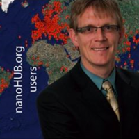
Gerhard Klimeck
Dr. Gerhard Klimeck is the Elmore Professor of Electrical and Computer Engineering at Purdue University; Director of the Network for Computational Nanotechnology; Reilly Director of the Center for Predictive Materials and Devices, Associate Vice President for Faculty IT Support, and Deputy CIO. He helped to create nanoHUB.org, the largest virtual nanotechnology user facility serving over 1.0 million global users, annually. Dr. Klimeck is a fellow of the Institute of Physics (IOP), the American Physical Society (APS), the Institute of Electrical and Electronics Engineers (IEEE), the American Association for the Advancement of Science (AAAS), and the German Humboldt Foundation. He has published over 540 printed scientific articles which are cited in over 23,000 times resulting in an h-index of 74 on Google Scholar. He has been recognized for his co-invention of a single-atom transistor, quantum mechanical modeling theory, and simulation tools. His NEMO5 software has been used since 2015 at Intel to design nano-scaled design transistors. The nanoHUB team was recently recognized by a top 100 by R&D award – Making simulation and data pervasive.
Gerhard Klimeck, Tanya Faltens, Daniel Mejia, Alejandro Strachan, Lynn Zentner, Michael Zentner*
Network for Computational Nanotechnology, Purdue University
*San Diego Supercomputing Center, UCSD
Gerhard Klimeck, Tanya Faltens, Daniel Mejia, Alejandro Strachan, Lynn Zentner, Michael Zentner*
Network for Computational Nanotechnology, Purdue University
*San Diego Supercomputing Center, UCSD

Gerhard Klimeck
Gerhard Klimeck
Dr. Gerhard Klimeck is the Elmore Professor of Electrical and Computer Engineering at Purdue University; Director of the Network for Computational Nanotechnology; Reilly Director of the Center for Predictive Materials and Devices, Associate Vice President for Faculty IT Support, and Deputy CIO. He helped to create nanoHUB.org, the largest virtual nanotechnology user facility serving over 1.0 million global users, annually. Dr. Klimeck is a fellow of the Institute of Physics (IOP), the American Physical Society (APS), the Institute of Electrical and Electronics Engineers (IEEE), the American Association for the Advancement of Science (AAAS), and the German Humboldt Foundation. He has published over 540 printed scientific articles which are cited in over 23,000 times resulting in an h-index of 74 on Google Scholar. He has been recognized for his co-invention of a single-atom transistor, quantum mechanical modeling theory, and simulation tools. His NEMO5 software has been used since 2015 at Intel to design nano-scaled design transistors. The nanoHUB team was recently recognized by a top 100 by R&D award – Making simulation and data pervasive.
Over 250,000 nanoHUB users have run over 7 million simulations in Apps mostly focused on semiconductor devices and materials modeling. nanoHUB created nano-Apps before Apple created Apps for the iPhone and made scientific codes usable for a much larger user group. Most scientific tools strive to be comprehensive in solving “any” simulation problem in a specific problem range. That comprehensiveness limits the use to experts, who require extensive training. nanoHUB has instead focused on delivering a spectrum of Apps (over 700 now) that individually have a limited capability focused on a PN-junction, MOSFET, or nanowire while the underlying tool could of course solve a much wider set of problems. We assembled some of these Apps that are essential for specific courses into small sets such as ABACUS (crystals, bandstructure, drift-diffusion, pn-junctions, BJTs, MOScaps, MOSFETs) [1]. The usability results are stunning. Our user analytics prove that over half of the simulation users participate in structured education through homework/project assignments. We can identify classroom sizes and detailed tool usage [2,3]. We can begin to build mind-maps of design explorations and assess depth of explorations for individuals and classes. While parts of academia struggled to innovate curricula, we have measured the median first-time App insertion into a class to be less than six months. Over 180 institutions have utilized nanoHUB in their curriculum innovation in over 3,600 classes. Over 1 million nanoHUB visitors explore lectures and tutorials annually. Based on this community presence we have expanded nanoHUB towards chip design. Chipshub.org deliver online modeling, simulation, virtual environments, and lectures for the US initiative on workforce development and research funded by the US CHIPSact. Commercial chip design vendors are partnering with Chipshub to host professional chip and semiconductor design software. This presentation will overview some of the nanoHUB impact metrics. In the tutorial a brief overview of ABACUS will be given and the audience may request other tool demonstrations or exploration.
[1] https://nanohub.org/groups/abacus ABACUS – Assembly of Basic Applications for Coordinated Understanding of Semiconductors. A one-stop-shop for teaching and learning semiconductor fundamentals.
[2] Krishna Madhavan, Michael Zentner, Gerhard Klimeck, “Learning and research in the cloud”, Nature Nanotechnology 8, 786–789 (2013)
[3] TEDx Talk, Klimeck, “Mythbusting Scientific Knowledge Transfer with nanoHUB.org”, https://www.youtube.com/watch?v=PK2GztIfJY4 .
Tutorial 2
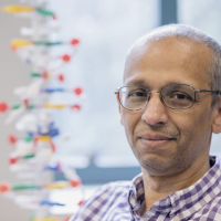
M. P. Anantram
M. P. Anantram
M. P. Anantram is a Professor of Electrical and Computer Engineering at the University of Washington, Seattle. Prior to this, he was a Professor at the University of Waterloo, Canada, and worked at the Center for Nanotechnology at the NASA Ames Research Center. His group works on algorithms and quantum mechanical methods to model biomolecules, nanoscale materials and devices. He recently co-authored a textbook titled Quantum Mechanics for Engineers and Material Scientists.
DNA Nanostructures – Insights from Electrical Modeling
M. P. Anantram
Department of Electrical and Computer Engineering
University of Washington, Seattle, WA, USA
DNA Nanostructures – Insights from Electrical Modeling
M. P. Anantram
Department of Electrical and Computer Engineering
University of Washington, Seattle, WA, USA

M. P. Anantram
M. P. Anantram
M. P. Anantram is a Professor of Electrical and Computer Engineering at the University of Washington, Seattle. Prior to this, he was a Professor at the University of Waterloo, Canada, and worked at the Center for Nanotechnology at the NASA Ames Research Center. His group works on algorithms and quantum mechanical methods to model biomolecules, nanoscale materials and devices. He recently co-authored a textbook titled Quantum Mechanics for Engineers and Material Scientists.
This tutorial serves as an introduction to the electronic properties of DNA and their heterostructures. DNA nanostructures exhibit precise self-assembly capabilities, forming heterostructures with high accuracy. These DNA heterostructures lay the groundwork for proposals involving memory elements, diodes, and resonant tunneling devices, which can emerge from either native DNA or through intercalation processes. We discuss DNA heterostructures of comparable lengths, which show a resistance contrast of nearly two orders of magnitude. Research on electronic transport also suggests the potential for an electrical method to identify short DNA strands, which could be instrumental in disease detection. We will explore the key components involved in modeling these heterostructures and provide an overview of our code for calculating their electronic properties. More recently, the construction of complex heterostructures based on the hybridization of multiple DNA strands has led to the development of 3D DNA nanostructures. These DNA architectures can be assembled into various shapes. We will discuss a recent proposal featuring a nanoscale pore for probing ionic concentration in cells when interfaced with transistors.
Another category of DNA nanostructures involving metal intercalation has been recently proposed by Vecchioni, Canary and Sha. These metal-intercalated structures introduce novel avenues for modulating the electronic properties of DNA. We will discuss the computational pathways for modeling these structures, along with the associated challenges. Modeling these structures necessitates a range of tools, from molecular dynamics to drift-diffusion simulators, depending on the specific features under study.
Tutorial 3
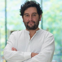
F. Pelayo García de Arquer
F. Pelayo García de Arquer
Pelayo García de Arquer is a Professor and group leader at ICFO, Barcelona. His research spans the engineering of nanostructured materials for applications in optoelectronics (photon sensors and sources, and thin-film photovoltaics), and energy storage using electrochemistry. His work has resulted in more than 120 peer reviewed publications, more than 29,000 lifetime citations and eight patents. Currently, his research group focuses on developing scalable and sustainable technologies for the production of chemicals, including green hydrogen and carbon dioxide capture and conversion.
Links:
Materials and system engineering in water and CO2 electrolysis
F. Pelayo García de Arquer
ICFO – The Institute of Photonic Sciences, Barcelona (Spain)
Materials and system engineering in water and CO2 electrolysis
F. Pelayo García de Arquer
ICFO – The Institute of Photonic Sciences, Barcelona (Spain)

F. Pelayo García de Arquer
F. Pelayo García de Arquer
Pelayo García de Arquer is a Professor and group leader at ICFO, Barcelona. His research spans the engineering of nanostructured materials for applications in optoelectronics (photon sensors and sources, and thin-film photovoltaics), and energy storage using electrochemistry. His work has resulted in more than 120 peer reviewed publications, more than 29,000 lifetime citations and eight patents. Currently, his research group focuses on developing scalable and sustainable technologies for the production of chemicals, including green hydrogen and carbon dioxide capture and conversion.
Links:
Electrolysis technologies such as water splitting, CO2 electroreduction, and other emerging reactions, present sustainable alternatives to power large industries such as transport (fuels), manufacturing (chemical feedstock) and agriculture (fertilizers). The viability of these technologies hinges upon achieving sufficient performance in metrics such as product selectivity, productivity (or current density), energy efficiency, and stability, at scale. Conventionally, improvements in these reactions have been sought by tuning the electronic and physicochemical properties of (pre)catalysts through compositional and structural modifications. Here, I will show engineering approaches to tune electrocatalytic activity in water and CO2 electrolysis by manipulating precatalyst reconstruction and reaction environment. I will discuss the need of tailored activation protocols and situ and operando spectroscopies at relevant working conditions to achieve reliability in catalyst design and operation. To conclude, I will overview sustainability issues in the scale up and path to market of CO2 electrolysis technologies.
Tutorial 4
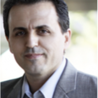
Ghassan E. Jabbour
M. P. Anantram
Professor Ghassan E. Jabbour holds the prestigious Tier 1 Canada Research Chair in Advanced Materials and Devices at the University of Ottawa, where he also serves as a professor in the School of Electrical Engineering and Computer Science, and the Biomedical Engineering Program. His work focuses on the green creation of nano and quantum materials and devices using reactive printing and coating approaches. A distinguished academic, Dr. Jabbour is a recipient of the SPIE Fellowship, a Fellow of the European Optical Society, and an honored Distinguished Professor by the Academy of Finland. He has delivered over 660 invited, keynote and plenary talks worldwide. He has directed research centers and garnered over $650 million in funding, with his achievements featured in leading scientific journals and recognized with multiple awards. Prof. Jabbour’s leadership extends across strategic university committees. Beyond academia, he enjoys the outdoors, cultural engagement, music, and the literary arts.
G.E. Jabbour
Faculty of Engineering, University of Ottawa, Ottawa (Canada)
G.E. Jabbour
Faculty of Engineering, University of Ottawa, Ottawa (Canada)

Ghassan E. Jabbour
Ghassan E. Jabbour
Professor Ghassan E. Jabbour holds the prestigious Tier 1 Canada Research Chair in Advanced Materials and Devices at the University of Ottawa, where he also serves as a professor in the School of Electrical Engineering and Computer Science, and the Biomedical Engineering Program. His work focuses on the green creation of nano and quantum materials and devices using reactive printing and coating approaches. A distinguished academic, Dr. Jabbour is a recipient of the SPIE Fellowship, a Fellow of the European Optical Society, and an honored Distinguished Professor by the Academy of Finland. He has delivered over 660 invited, keynote and plenary talks worldwide. He has directed research centers and garnered over $650 million in funding, with his achievements featured in leading scientific journals and recognized with multiple awards. Prof. Jabbour’s leadership extends across strategic university committees. Beyond academia, he enjoys the outdoors, cultural engagement, music, and the literary arts.
Gold nanoparticles (AuNPs) are crucial components in a wide range of applications, including catalysis, printed electronics, detecting systems, and intelligent packaging. This is due to their remarkable chemical, physical, and optical capabilities. Historically, the fabrication of AuNPs and their thin films and devices has necessitated intricate processes that demand sophisticated equipment such as mechanical milling, vacuum deposition, and lithography. These methods are primarily employed for expensive devices or small-scale samples. In contrast, solution-based procedures offer a more straightforward and cost-efficient option that is suitable for large-scale production. The speaker will presents a simple in-situ reduction reactive blade-coating method that is suitable for roll-to-roll coating and printing methods. This methodology allows for the production of films containing AuNPs on both rigid and flexible substrates. By manipulating the quantities of reactants and the solvent systems, we are able to create films of gold nanoparticles with different sizes and shapes. This technique facilitates the production of flexible, printable devices using AuNPs technology in a more cost-effective manner, suitable for applications in the fields of electronics, photonics, chemistry, and biomedicine.
